© National Instruments Corporation 17 NI 5421 Specifications
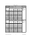
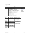
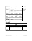
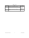
Onboard Clock
(Internal VCXO)
Sample Clock Exporting
Exported
Sample Clock
Destinations
1. PFI<0..1> (SMB front panel connectors)
2. DDC CLK OUT (DIGITAL DATA & CONTROL front
panel connector)
3. NI PXI-5421—PXI_Trig<0..7> (backplane connector)
NI PCI-5421—RTSI<0..7>
Exported Sample
Clocks can be
divided by integer
K (1 ≤ K ≤
4,194,304).
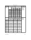
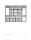
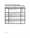
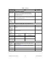
Exported
Sample Clock
Destinations
Maximum
Frequency
Jitter (Typical) Duty Cycle
—
PFI<0..1> 105 MHz PFI 0: 6 ps rms
PFI 1: 12 ps rms
25% to 65%
DDC CLK
OUT
105 MHz 40 ps rms 40% to 60%
NI PXI-5421
PXI_Trig<0..7>
20 MHz — —
NI PCI-5421
RTSI<0..7>
20 MHz — —
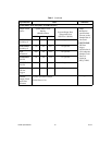
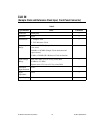
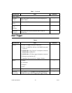
Table 3.
Specification Value Comments
Clock Source Internal sample clocks can either be locked to a Reference
Clock using a phase-locked loop or be derived from the
onboard VCXO frequency reference.
—
Frequency
Accuracy
±25 ppm —
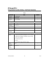
Table 2. (Continued)
Specification Value Comments


