


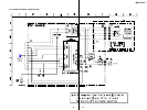

57
MDS-JE770
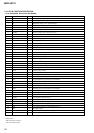
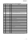
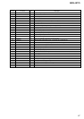
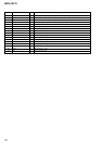
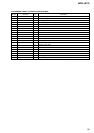
40 ADA. LATCH O Chip select signal output to the AK4524. L: Active
41 EPN I Not used. (Fixed at L)
42 L : DINT1/H : CLIP — Not used. (open)
43 NC — Not used.
44 PROTECT I Recording-protection claw detection input from the protection detection switch. H: Protect
45 SCL O Clock signal output to the EEP-ROM.
46 CE I Not used. (Fixed at H)
47 EEP-WP O EEP-ROM write protect signal output. L: write possibility
48 XBUSY I Busy signal input from the CXD2662R
49 OUT-SW I Detection signal input from the loading out detection switch.
50 XLATCH O Latch signal output to CXD2662R.
51 PLAY-SW I Detection signal input from the playback position detection switch. L: PLAY
52 DIG-RST O Digital rest signal output to the CXD2662R and motor driver. L: Reset
53 REC-SW I Detection signal input from the recording position detection switch. L: REC
54 WR PWR O Laser power ON/OFF signal output. L: PLAY H: REC
55 LIMIT-IN I Detection input from the limit switch. L: Sled limit-In H: Sled limit-Out
56 MOD O Laser modulation switching signal output. (L: STOP, H : PLAY, pluse : REC)
57 LDON O Laser ON/OFF control output. H: Laser ON
58 SENS I Internal status (SENSE) input from the CXD2662R.
59 SHOCK I Track jump signal input from the CXD2662R.
60 SDA I/O Data signal input/output pin with the EEP-ROM.
61 REFLECT I Disk reflection rate detection input from the reflect detection switch. H: Disk with low reflection rate.
62 VCC I Power supply. (+3.3V)
63 NC — Not used.
64 GND — Ground.
65 LOAD LO O Loading motor voltage control output
66 LOAD OUT O Loading motor control output. H: eject
67 LOAD IN O Loading motor control output. H: loading
68 - 71 MODEL SEL 0 - 3 — Not used.
72 - 80 NC — Not used.
DescriptionPin Name
Pin No.
I/O