


Si85xx-TB UG
Confidential Rev. 0.1 3
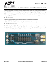
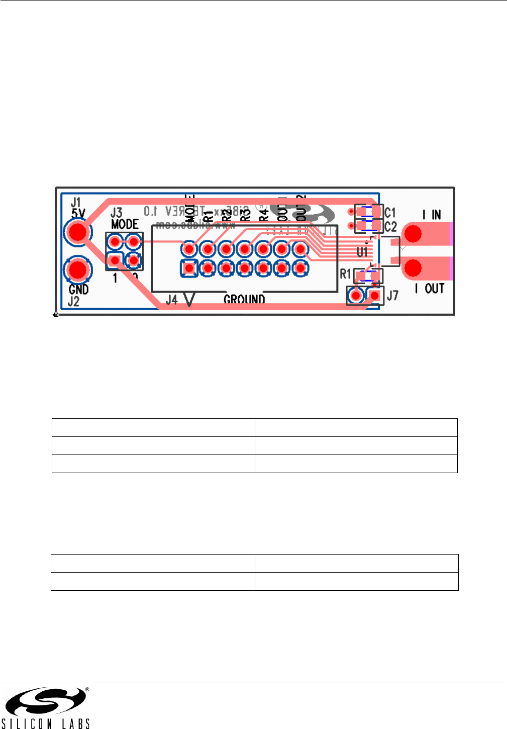
4. Si85xx Evaluation Board
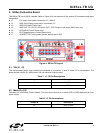
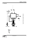
The Si85xx-TB has a Si8512 installed. Refer to Figure 4 for the locations of the various I/O connectors and major
components.
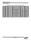
J1 5 V Supply Input power connection 5 V, 100 mA
J2 GND, Input Supply power return connection, 0 V
J3 HDR-2X2, Mode Control input
J4 HDR-2X07, R1, R2, R3, R4 inputs, OUT1, OUT2 outputs, and seven GND return pins
J5 IIN Positive Current Sense Input
J6 IOUT Negative/return Current Sense Input
J7 HEADER, TRST timing select jumper, default tied to VDD
Figure 4. Si85xx-TB Layout
4.1. VIN (J1, J2)
The user-provided power supply should be connected to connectors J1 and J2 where J2 is the reference. The
power source must be 5 V with at least 100 mA maximum output current.
4.2. Mode Pin (J3)
Connector J3 is the Mode Control header. The user should tie this pin to either VDD or GND depending on their
power supply.
Table 1. J1, J2 Pin Descriptions
Jumper # Description
J1 5 V, 100 mA
J2 GND
Table 2. J3 Pin Descriptions
Jumper # Description
J3 VDD or GND